- 您现在的位置:买卖IC网 > Sheet目录230 > IP4350CX24/LF,135 (NXP Semiconductors)IC ESD PROTECT SD MEMORY 24WLCSP
NXP Semiconductors
Table 1.
IP4350CX24
9-channel SD memory card interface ESD protection ?lter
Pin description …continued
Symbol
DATA1
DATA0
GND_C
SDDATA1
SDDATA0
Pin
E1
E2
E3
E4
E5
Type [1]
I/O
I/O
S
I/O
I/O
Description
data 1 input or output
data 0 input or output
card supply ground
data 1 input or output on SD card side
data 0 input or output on SD card side
[1]
I = input, O = output, I/O = input and output, S = power supply.
3. Ordering information
Table 2.
Ordering information
Type number
Package
Name
Description
Version
IP4350CX24
WLCSP24
wafer level chip-size package; 24 bumps; 1.95 × 2.11 × 0.61 mm
IP4350CX24/LF
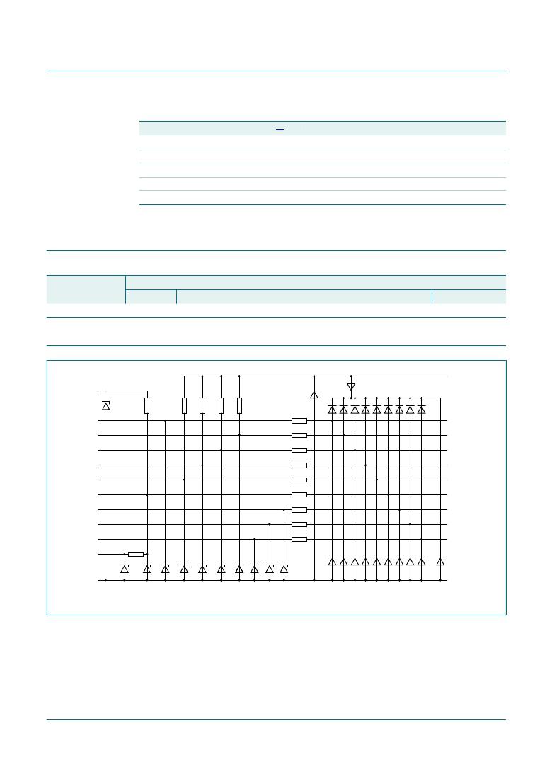
4. Functional diagram
VSD
DAT3_PU
R11
R12
R13
R14
R15
R1
CLK
CMD
DATA0
DATA1
DATA2
DATA3
CD
WP
WP+CD
DAT3_PD
GND_H
R21
R2
R3
R4
R5
R6
R7
R8
R9
SDCLK
SDCMD
SDDATA0
SDDATA1
SDDATA2
SDDATA3
SDCD
SDWP
SDWP+CD
GND_C
001aaj750
Fig 2.
IP4350CX24_1
Schematic diagram IP4350CX24
? NXP B.V. 2010. All rights reserved.
Product data sheet
Rev. 01 — 5 February 2010
3 of 16
发布紧急采购,3分钟左右您将得到回复。
相关PDF资料
IP4352CX24/LF,135
DIODE ARRAY ESD PROT 9CH WLCSP24
IP4358CX6,135
IC ESD PROTECTION
IP4387CX4/P,315
IC ESD PROTECTION WLCSP
IP4790CZ38/1,118
IC ESD PROTECTION VIDEO 38TSSOP
IPC3SAD7/1L0G
SWITCH PUSH SPST-NO 0.5A 48V
IPR1SAD2L0G
SWITCH PUSHBUTTON SPST 2A 125V
IPS-3901
BOX ALUM 3.79X3.79X1.77 NAT
IPS-3903
BOX ALUM 3.79X3.79X2.64 NAT
相关代理商/技术参数
IP4352CX24
制造商:PHILIPS 制造商全称:NXP Semiconductors 功能描述:9-channel SD memory card interface filter with ESD protection to IEC 61000-4-2 level 4
IP4352CX24/LF
制造商:PHILIPS 制造商全称:NXP Semiconductors 功能描述:9-channel SD memory card interface filter with ESD protection to IEC 61000-4-2 level 4
IP4352CX24/LF,135
功能描述:ESD 抑制器 9CH SD MEMORY CARD RoHS:否 制造商:STMicroelectronics 通道:8 Channels 击穿电压:8 V 电容:45 pF 端接类型:SMD/SMT 封装 / 箱体:uQFN-16 功率耗散 Pd: 工作温度范围:- 40 C to + 85 C
IP4353CX15/LF
制造商:NXP Semiconductors 功能描述:Cut Tape
IP4353CX15/LF,135
功能描述:ESD 抑制器 6-CH CRC-type EMI filter/ESD protect RoHS:否 制造商:STMicroelectronics 通道:8 Channels 击穿电压:8 V 电容:45 pF 端接类型:SMD/SMT 封装 / 箱体:uQFN-16 功率耗散 Pd: 工作温度范围:- 40 C to + 85 C
IP4355CX6/LF
制造商:NXP Semiconductors 功能描述:
IP4355CX6/LF,135
功能描述:ESD 抑制器 Audio pathEMI Filter ESD protect devices RoHS:否 制造商:STMicroelectronics 通道:8 Channels 击穿电压:8 V 电容:45 pF 端接类型:SMD/SMT 封装 / 箱体:uQFN-16 功率耗散 Pd: 工作温度范围:- 40 C to + 85 C
IP4355CX6/P,135
制造商:NXP Semiconductors 功能描述:- Tape and Reel
